|


| |
Introduction
Structures with periodicity in three dimensions can be
constructed so that they posses an omnidirectional photonic bandap.
Light with frequencies lying within this band gap cannot propagate
regardless of polarization and incidence angle. By locally altering the
crystal properties, one may engineer a "defect" in such a way to allow a defect
mode to exist within the band gap. Since the defect is surrounded by the
periodic material possessing an omnidirectional bandgap, the light is
confined to the defect region.
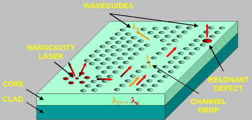
If one creates a linear defect region, it
can
propagate light like a wave guide. Unlike conventional wave guides, a
photonic crystal wave guide can be constructed to allow sharp bends without
loss. Similarly, a point defect will act as a resonator. Add some active
material and you can create micro-sized amplifiers and lasers. If you add
variable index material to branching waveguides, you can create a switch.
Combining resonators and wave guides, you create add/drop multiplexers, and
so on. All sorts of optical circuit devices have been proposed. Below is an
artist's rendition of such a optical chip. The drawing is a conceptual
illustration only, and not to any sort of scale.
|
 |
|
Unfortunately, 3D crystals are hard to
manufacture. Some promising work with self-assembling crystals is underway, but defect
creation has been a problem until recently. Personally, I don't work with
self-assembling crystals because the field requires a strong background in
chemistry (which I lack). The other method of constructing photonic crystals
is through photolithography. Photolithography works very well with planar
processes, so most of the research using the photolithographic process center on
photonic crystal slabs. A slab has periodicity in two dimensions (say
the x & y directions), and uses TIR confinement in the third dimension (the
z direction) by utilizing a lower index cladding above and below the slab.
Most of my recent work has been with slab structures. |
Modeling and Simulation
Frequency Domain
Calculations - The first step in modeling a photonic crystal is to produce a dispersion diagram of
the crystal with no defects present. This determines if a band gap exists, and if so, its size and location in frequency. Once that
information is determined, a dispersion diagram of the defect is
constructed.
Time Domain Calculations
- In order to find the transmission properties of the photonic crystal with
its defect structure, one uses finite-difference time domain calculations.
With FDTD, one can find the transmission properties of a photonic
crystal waveguide, including transmission around sharp bends. FDTD can also
account for material losses. But most importantly, the transmission results
can be compared directly to experimental results.
Parallel Computing with FDTD
- I begin most calculations in 2D (periodicity in the x & y directions with
z assumed to be uniform). This gives a rough estimate of the photonic
crystal properties with minimal computational requirements. However,
modeling the full 3D problem with FDTD requires enormous computational
resources. Fortunately, FDTD is well suited to parallel computing
techniques.
Photonic
Crystal Boundary Conditions with FDTD - Photonic crystals require
special considerations when terminating the FDTD computational domain. |
Miscellaneous
Links to other Photonic Crystal
Websites - Here are some links to websites which I frequently visit
related to photonic crystals. |
|